if the two drain currents do not match explain what will happen to the output voltage
VLSI Design - MOS Inverter
The inverter is truly the nucleus of all digital designs. One time its operation and properties are clearly understood, designing more than intricate structures such equally NAND gates, adders, multipliers, and microprocessors is greatly simplified. The electrical beliefs of these circuitous circuits can be virtually completely derived by extrapolating the results obtained for inverters.
The analysis of inverters can be extended to explain the beliefs of more circuitous gates such as NAND, NOR, or XOR, which in plow form the building blocks for modules such as multipliers and processors. In this chapter, nosotros focus on one single incarnation of the inverter gate, being the static CMOS inverter — or the CMOS inverter, in short. This is certainly the nearly popular at present and therefore deserves our special attention.
Principle of Functioning
The logic symbol and truth tabular array of platonic inverter is shown in figure given below. Here A is the input and B is the inverted output represented by their node voltages. Using positive logic, the Boolean value of logic ane is represented past V dd and logic 0 is represented by 0. 5 th is the inverter threshold voltage, which is Five dd /two, where Five dd is the output voltage.
The output is switched from 0 to V dd when input is less than V th . Then, for 0<V in <V thursday output is equal to logic 0 input and V th <Five in < V dd is equal to logic 1 input for inverter.
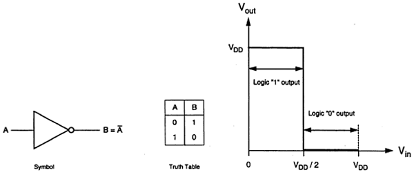
The characteristics shown in the figure are ideal. The generalized circuit construction of an nMOS inverter is shown in the figure beneath.
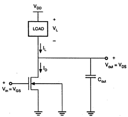
From the given figure, we can meet that the input voltage of inverter is equal to the gate to source voltage of nMOS transistor and output voltage of inverter is equal to bleed to source voltage of nMOS transistor. The source to substrate voltage of nMOS is also called driver for transistor which is grounded; and then V SS = 0. The output node is continued with a lumped capacitance used for VTC.
Resistive Load Inverter
The basic structure of a resistive load inverter is shown in the effigy given below. Here, enhancement type nMOS acts as the commuter transistor. The load consists of a unproblematic linear resistor R L . The power supply of the circuit is Five DD and the bleed electric current I D is equal to the load current I R .
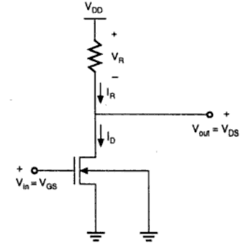
Circuit Performance
When the input of the driver transistor is less than threshold voltage Five Thursday (V in < V Th ), commuter transistor is in the cut – off region and does not conduct whatever current. So, the voltage drop across the load resistor is Null and output voltage is equal to the V DD . Now, when the input voltage increases farther, commuter transistor volition start conducting the non-zip current and nMOS goes in saturation region.
Mathematically,
$$I_{D} = \frac{K_{north}}{ii}\left [ V_{GS}-V_{TO} \right ]^{2}$$
Increasing the input voltage further, commuter transistor will enter into the linear region and output of the driver transistor decreases.
$$I_{D} = \frac{K_{n}}{2}2\left [ V_{GS}-V_{TO} \correct ]V_{DS}-V_{DS}^{2}$$
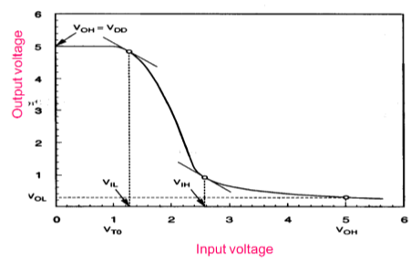
VTC of the resistive load inverter, shown below, indicates the operating mode of driver transistor and voltage points.
Inverter with N type MOSFET Load
The main reward of using MOSFET as load device is that the silicon area occupied by the transistor is smaller than the expanse occupied past the resistive load. Here, MOSFET is agile load and inverter with active load gives a improve performance than the inverter with resistive load.
Enhancement Load NMOS
Two inverters with enhancement-type load device are shown in the figure. Load transistor can exist operated either, in saturation region or in linear region, depending on the bias voltage practical to its gate terminal. The saturated enhancement load inverter is shown in the fig. (a). It requires a single voltage supply and simple fabrication procedure and and so Five OH is limited to the V DD − V T .
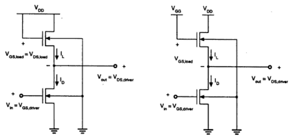
The linear enhancement load inverter is shown in the fig. (b). It ever operates in linear region; so V OH level is equal to V DD .
Linear load inverter has higher noise margin compared to the saturated enhancement inverter. Just, the disadvantage of linear enhancement inverter is, it requires 2 divide power supply and both the circuits suffer from loftier power dissipation. Therefore, enhancement inverters are not used in any large-scale digital applications.
Depletion Load NMOS
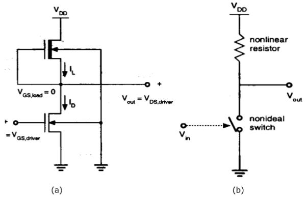
Drawbacks of the enhancement load inverter can exist overcome by using depletion load inverter. Compared to enhancement load inverter, depletion load inverter requires few more than fabrication steps for channel implant to arrange the threshold voltage of load.
The advantages of the depletion load inverter are - precipitous VTC transition, better noise margin, unmarried ability supply and smaller overall layout expanse.
As shown in the figure, the gate and source terminal of load are connected; And so, V GS = 0. Thus, the threshold voltage of the load is negative. Hence,
$$V_{GS,load}> V_{T,load}$$ is satisfied
Therefore, load device always has a conduction channel regardless of input and output voltage level.
When the load transistor is in saturation region, the load electric current is given by
$$I_{D,load} = \frac{K_{north,load}}{2}\left [ -V_{T,load}\left ( V_{out} \right ) \right ]^{2}$$
When the load transistor is in linear region, the load current is given by
$$I_{D,load} = \frac{K_{n,load}}{two}\left [ 2\left | V_{T,load}\left ( V_{out} \correct ) \right |.\left ( V_{DD}-V_{out} \right )-\left ( V_{DD}-V_{out} \right )^{2} \right ]$$
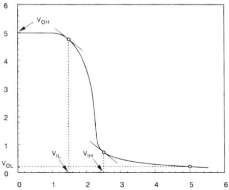
The voltage transfer characteristics of the depletion load inverter is shown in the figure given below −
CMOS Inverter – Circuit, Performance and Description
The CMOS inverter circuit is shown in the figure. Here, nMOS and pMOS transistors work as driver transistors; when one transistor is ON, other is OFF.
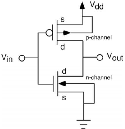
This configuration is called complementary MOS (CMOS). The input is continued to the gate last of both the transistors such that both tin can be driven directly with input voltages. Substrate of the nMOS is continued to the footing and substrate of the pMOS is connected to the power supply, 5 DD .
So V SB = 0 for both the transistors.
$$V_{GS,northward}=V_{in}$$
$$V_{DS,n}=V_{out}$$
And,
$$V_{GS,p}=V_{in}-V_{DD}$$
$$V_{DS,p}=V_{out}-V_{DD}$$
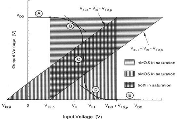
When the input of nMOS is smaller than the threshold voltage (V in < V TO,northward ), the nMOS is cut – off and pMOS is in linear region. So, the drain current of both the transistors is cypher.
$$I_{D,n}=I_{D,p}=0$$
Therefore, the output voltage Five OH is equal to the supply voltage.
$$V_{out}=V_{OH}=V_{DD}$$
When the input voltage is greater than the V DD + 5 TO,p , the pMOS transistor is in the cutoff region and the nMOS is in the linear region, then the drain current of both the transistors is cypher.
$$I_{D,due north}=I_{D,p}=0$$
Therefore, the output voltage V OL is equal to null.
$$V_{out}=V_{OL}=0$$
The nMOS operates in the saturation region if V in > 5 TO and if following weather are satisfied.
$$V_{DS,n}\geq V_{GS,northward}-V_{TO,northward} $$
$$V_{out}\geq V_{in}-V_{TO,n} $$
The pMOS operates in the saturation region if V in < Five DD + Five TO,p and if following conditions are satisfied.
$$V_{DS,p}\leq V_{GS,p}-V_{TO,p} $$
$$V_{out}\leq V_{in}-V_{TO,p} $$
For different value of input voltages, the operating regions are listed below for both transistors.
| Region | Five in | V out | nMOS | pMOS |
|---|---|---|---|---|
| A | < V TO, n | V OH | Cutting – off | Linear |
| B | V IL | High ≈ V OH | Saturation | Linear |
| C | 5 thursday | V th | Saturation | Saturation |
| D | V IH | Low ≈ V OL | Linear | Saturation |
| E | > (V DD + V TO, p ) | Five OL | Linear | Cut – off |
The VTC of CMOS is shown in the figure beneath −
Useful Video Courses

Video

Video
Source: https://www.tutorialspoint.com/vlsi_design/vlsi_design_mos_inverter.htm
0 Response to "if the two drain currents do not match explain what will happen to the output voltage"
Post a Comment